...

Xallent – Advanced Nanoscale Testing Solutions

nezer5

Xallent Successfully Installs Fine-Pitch Testing System in Dubai, UAE

Xallent Successfully Installs Fine-Pitch Testing System in Dubai, UAE September 29, 2025 | ALBANY, NY – Xallent has successfully completed the installation and training of its SAKYIWA NanoProber system at at a prominent high-tech company in Dubai, UAE. This advanced tool is designed to provide crucial early insights into advanced materials, which will be instrumental in the development of smart contact lenses for both extended reality (XR) and health monitoring applications. We are confident that this installation will significantly contribute to our client’s innovative work in these cutting-edge fields.

Xallent Successfully Installs Fine-Pitch Testing System in Dubai, UAE Read More »

Xallent Collaborates with IBM on Advanced Package Tests

Xallent Collaborates with IBM on Advanced Package Tests June 7, 2025 | ALBANY, NY –Xallent made a significant splash at SWTest 2025! We presented groundbreaking findings from our collaborative work with IBM on “Fine Pitch Probing of Micro-Bumps for Advanced Packages.” This project showcased the power of our 𝗳𝗶𝗻𝗲 𝗽𝗶𝘁𝗰𝗵 (𝟭𝟬 µ𝗺) 𝗞𝗲𝗹𝘃𝗶𝗻 𝗽𝗿𝗼𝗯𝗲𝘀 𝗮𝗻𝗱 𝗛𝗲𝘁𝗲𝗿𝗼𝗴𝗲𝗻𝗲𝗼𝘂𝘀 𝗜𝗻𝘁𝗲𝗴𝗿𝗮𝘁𝗶𝗼𝗻 𝗧𝗲𝘀𝘁 𝗦𝘆𝘀𝘁𝗲𝗺 (𝗛𝗜𝗧𝗦™), enabling us to precisely measure the resistance of individual micro-bumps on a 300mm wafer. This innovative probing solution delivers vital early insights into advanced packaging processes, directly contributing to maximized yields and a faster time-to-market for cutting-edge 𝗔𝗜 𝗰𝗵𝗶𝗽𝘀.

Xallent Collaborates with IBM on Advanced Package Tests Read More »

Xallent Successfully Installs Fine-Pitch Testing System at ASU’s Defense Microelectronics Hub

Xallent Successfully Installs Fine-Pitch Testing System at ASU’s Defense Microelectronics Hub April 4, 2025 | ALBANY, NY – Xallent has successfully completed the installation and training of its SAKYIWA NanoProber system at the Arizona State University’s Southwest Advanced Prototyping (SWAP) Hub. SWAP is a critical partner, serving as one of eight regional innovation hubs supported by the Department of Defense’s Microelectronics Commons. This national initiative is designed to accelerate the development and production of microelectronics vital to U.S. security and defense. The SAKYIWA NanoProber utilizes advanced 10-micrometer pitch 4-point probes for the rapid, economical measurement of sheet resistance in thin films and 2D materials. This cutting-edge technology will empower SWAP researchers to dramatically shorten learning cycles by reducing essential testing times from over 12 hours to under 5 minutes, rapidly accelerating key microelectronics innovations for national security.  

Xallent Successfully Installs Fine-Pitch Testing System at ASU’s Defense Microelectronics Hub Read More »

Xallent & MPI Announce Strategic Partnership

Xallent and MPI Announce Strategic Partnership to Innovate and Accelerate the Development of Next Generation AI Chips January 15, 2025 | ALBANY, NY – Xallent Inc., a global leader in fine pitch probing and MPI Corporation, a global leader in advanced semiconductor tests, today announced their strategic partnership and launch of the Heterogeneous Integration Test System (HITSTM). The HITSTM is a semi-automatic test system for chiplets, advanced packages, and thin film materials tests. The HITSTM leverages Xallent’s fine pitch probe cards, automation software, and MPI’s automated probe systems to more rapidly provide early actionable insights into chiplet manufacturing, advanced packaging, and thin film materials. The HITSTM supports wafer sizes ranging from 300 mm to pieces. Advances in artificial intelligence (AI), high performance computing (HPC), and high bandwidth memory (HBM) will transform our lives. Advanced computing chips are being developed which will lead to profound societal and commercial impacts. As Moore’s Law scaling becomes more and more challenging, advanced packaging is the path forward for the semiconductor industry to keep pace. Chiplets will play an outsized role in addressing some of the challenges. However, it is prohibitively expensive for chipmakers and integrators to heterogeneously integrate faulty chiplets, as a single faulty chiplet could render an entire system-in-package useless at significant cost, time, and effort. Thus, it is imperative that chiplets are faultless, requiring testing innovations to monitor chiplet manufacturing and assembly processes. “The probing paradigm enabled by the HITSTM will have far-reaching commercial and societal impacts, magnified by the powerful trends driving mobility, connectivity, and enterprise,” said Xallent CEO & founder Dr. Kwame Amponsah. “The HITSTM will provide early actionable insights into known-good-die, determine potential process variations which could significantly reduce chiplet design costs by 25% while accelerating time-to-market by up to 3 months.” “This partnership leverages MPI’s expertise in automated probing systems and Xallent’s patented fine pitch probe cards and advanced software. Together, these technologies create a unified platform that enables precise, high-throughput testing of chiplets and advanced packages. By combining MPI’s reliable automation and Xallent’s innovative probing solutions, the HITS™ empowers customers to achieve greater accuracy, faster results, and cost efficiencies in chiplet and heterogeneous integration development. We are pleased to strengthen our strategic partnership with Xallent and to continue our joint efforts to innovate and accelerate the development of next-generation AI chips,” said Dr. Stojan Kanev, General Manager, MPI-Advanced Semiconductor Test Division. About Xallent A global leader in fine pitch probing, Xallent Inc. designs, develops, manufactures, and markets advanced hardware and software tools for micro and nanoscale probing measurements. Xallent’s patented fine pitch probe cards and test systems are used for the most demanding testing applications of chiplets, advanced packages, and thin film materials. As the semiconductor industry pushes the design frontier, Xallent’s technologies enable industry-leading research labs and production facilities to dramatically improve their measurement and analytics capabilities with greater accuracy, speed, and at lower costs. Xallent is headquartered at the Albany Nanotech Complex in Albany, New York, USA. About MPI Founded in 1995 and headquartered in Hsinchu, Taiwan, MPI Corporation is a global technology leader in the testing of semiconductors, light emitting diodes (LED), photo detectors, lasers, materials research, aerospace, automotive, fiber optic, electronic components, and more. MPI offers a wide-ranging portfolio of products and services, from advanced probe card technologies, mass production and engineering probe systems, testers, material handlers, inspection systems, and thermal air stream systems. Many of these products are accompanied by state-of-the-art calibration and test & measurement software suites.

Xallent & MPI Announce Strategic Partnership Read More »

Air Force Research Labs Collaborates with Xallent

November 18, 2024 | ALBANY, NY – Advances in radar, hypersonic systems, radiation-hard space applications, and the need for continuous improvements in Size, Weight, and Power (SWaP), necessitate materials that can support higher voltages, temperatures, frequencies, and power densities than silicon. Wide bandgap (WBG) materials meet these requirements. Xallent, in collaboration with the Air Force Research Laboratory (AFRL) will develop a non-destructive testing methodology to more rapidly screen WBG materials. The funding award for this initiative was announced at the recent AFRL Regional Network – Mid-Atlantic Annual Meeting held on November 7, 2024.

Air Force Research Labs Collaborates with Xallent Read More »

NIST and Xallent Teams Up to Develop a Nanomachine Probe

September 27, 2024 | ALBANY, NY – Xallent’s collaboration with the National Institute of Standards and Technology (NIST) has resulted in a novel nanomachine probe. The probe leverages nano-electro-mechanical-systems (NEMS) technology and is monolithically integrated with sensors, actuators, and a high aspect ratio nanoscale probe tip. This probe is poised to advance the development of through-silicon-vias (TSV), microbumps, and hybrid bond pads for high performance computing (HPC) and high bandwidth memory (HBM) applications.

NIST and Xallent Teams Up to Develop a Nanomachine Probe Read More »

Xallent Moves Headquarters to Albany

February 23, 2024 | ALBANY, NY – To advance our organizational goals and better contribute to the semiconductor industry, we are thrilled to announce the relocation of Xallent’s headquarters from Ithaca, New York to Albany, New York. This strategic move co-locates our organization with our marquee clients and partners at the Albany Nanotech Complex. The complex houses 300 mm wafer production lines and will house North America’s first and only publicly owned high NA extreme ultraviolet lithography center. We look forward to leveraging the advanced semiconductor and MEMS processing resources onsite to advance our research and commercialization objectives.

Xallent Moves Headquarters to Albany Read More »

Semiconductor Wafer Test Receives Substantial Boost

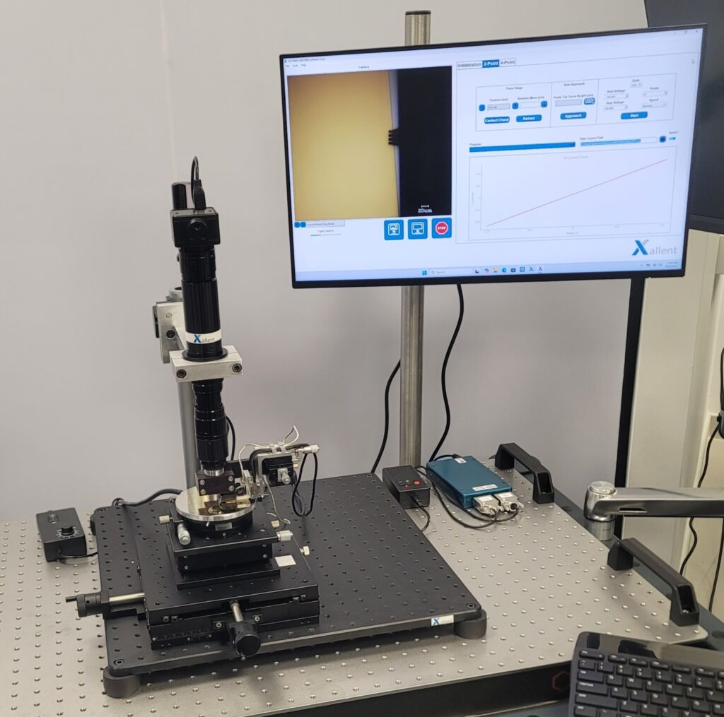
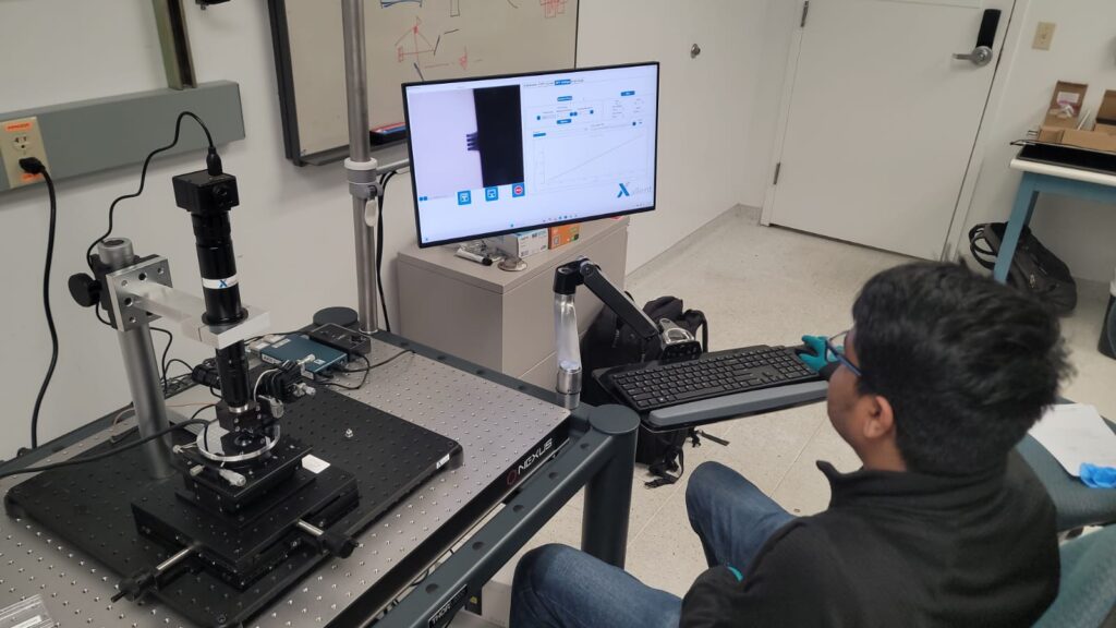
ITHACA, NY –  Efforts to push the frontiers of nanoscale chip design received a significant boost today when Xallent, a world leader in nanoscale measuring solutions, today announced pre-orders for their next-generation SAKYIWA system, which features probes 1800X smaller than the current market standard. In addition to smaller probes, the Xallent system speeds up common measurement workflows by 300X, semi-automates repeated measurements, minimizes tedious sample preparation, and provides much higher accuracy measurements of smaller samples. Making consumer electronics smaller, faster, and more powerful depends to a large degree on the ability of the semiconductor industry to create chip designs with smaller design parameters. Currently in volume production is 5 nanometers, but researchers are working on 3 nm, 2 nm, and even 1.4 nm designs, which will be crucial to achieving the promise of technologies such as 6G, autonomous vehicles, and augmented reality wearables. One of the key limitations has been the inability to easily and reliably measure prototypes produced at these small sizes. “Our Xallent system has given our user base several orders-of-magnitude improvement in measurement throughput and drastically decreased their cost of testing,” says Ron Olson, the Director of Operations at the Cornell NanoScale Facility, the first customer for the new technology. “The Xallent system represents a key milestone in semiconductor and thin film materials characterization.” The Xallent system is used for DC, high frequency, CV electrical testing, mechanical and scanning probe testing, imaging, and metrology. Measuring the electrical and mechanical properties of thin film materials, MEMS, photonics, and solid-state devices at the micro and nanoscale can now be done on the same system, faster, with higher resolution, and at a fraction of the cost. The new SAKYIWA system replaces measurement equipment that costs about 5 times as much and takes up 10 times the lab space. “Today’s announcement is the result of years of research and development, and it’s a huge moment for the entire Xallent team,” said Xallent founder and CEO Dr. Kwame Amponsah. Funded in part via grants and partnerships with U.S. Government and New York State agencies including Defense Advanced Research Projects Agency (DARPA), National Science Foundation (NSF), National Institute of Standards and Technology (NIST), and the U.S. Army, the Xallent technology will help realize the promise of emerging high performance computing technologies. The Xallent system announced today offers a complete solution including probes, probe heads, the wafer prober, and the AI-powered software to run it. For research labs and production facilities that already have substantial hardware investments, Xallent also announced a probe head that works as a drop-in replacement for manipulators on conventional systems and that immediately enables many of the Xallent benefits with essentially no hardware investment. More information about the products and the company can be found at the newly re-designed website www.xallent.com. About XallentXallent LLC designs, develops, manufactures, and markets the world’s most advanced hardware and software tools for micro and nanoscale probing measurements. Xallent’s patented probe cards, probe heads, and wafer probers are used for the most demanding applications in the imaging, electrical, and mechanical testing of semiconductor devices and thin film materials, and enable industry-leading research labs and production facilities to dramatically improve their measurement and analytics capabilities with greater accuracy, speed, and at a lower cost. Xallent was founded by Dr. Kwame Amponsah together with Dr. Amit Lal, and Dr. Ashish Kumar at Cornell University in 2013. The technology was refined and commercialized through grants, partnerships, and contracts with DARPA, NSF, NIST, the U.S. Army, Sandia National Laboratory, Brookhaven National Laboratory, the Cornell NanoScale Facility, University of Michigan, University of Pennsylvania, and NY State. Xallent is headquartered in Ithaca, New York.

Semiconductor Wafer Test Receives Substantial Boost Read More »

Xallent Partners with Microsoft under the Microsoft StartUp Program

ITHACA, NY – Xallent is happy to announce that it has been selected to be part of Microsoft’s highly competitive early-stage B2B Startup program! This program aims at creating technical solutions that support customers in their digital transformation. As part of this program, we have received access to free Microsoft cloud technologies, including Azure credits, along with tech support and guidance which will be pivotal in developing innovative solutions. This partnership with Microsoft will help us to incorporate Artificial Intelligence and Machine Learning tools to build solutions that will have a far-reaching impact on our customers. We also get a chance to collaborate and sell our solutions through Microsoft’s Commercial Market place which will aid in building our brand and improve our brand recognition in the nanoscale testing solutions market. Xallent LLC is in the process of scaling the organization and teaming up with Microsoft will provide the platform to connect with larger players in the semiconductor market to support our endeavor of solving customer’s problems based on their business needs.

Xallent Partners with Microsoft under the Microsoft StartUp Program Read More »

Xallent Came Third in BenDaniel Venture Challenge

ITHACA, NY – Xallent LLC, the manufacturer of solutions and equipment for testing semiconductors and thin film materials at the nanoscale, came third in the BenDaniel Venture Challenge (Cornell Venture Challenge). As one of the nation’s most active MBA student-run venture capital funds, Big Red Ventures (BRV) has been sponsoring the Cornell Venture Challenge since the year 2009. This March, the BRV fund managers set up stringent judging criteria and ran through 70+ applications of Cornell-affiliated ventures. The purpose of the challenge is to provide an opportunity for burgeoning entrepreneurs to gain experience, exposure, and financing to help develop their business ideas to actionable and high-impact ventures. Winnowing the applications into a list of finalists was a herculean task. The finalists selected for this year represent ideas from different parts of the Cornell community and have the potential to make a lasting impact on the future.

Xallent Came Third in BenDaniel Venture Challenge Read More »

Seraphinite AcceleratorOptimized by Seraphinite Accelerator
Turns on site high speed to be attractive for people and search engines.