 Skip to content
Services
.
Custom Probes and More
Custom probe development can take months and even years. Why not leverage our expertise in NEMS and MEMS to accelerate your work? Xallent offers services in probe design, manufacturing, packaging, and testing. We have extensive experience with customers in research, IC chip manufacturing, defense, healthcare, automotive, and consumer electronics. Our expertise includes:
- NEMS & MEMS Probe Design: We ensure that the anticipated probe device is designed for manufacturability (DFM).
- Finite Element Analysis (FEA): Our engineers perform FEA analyses on CAD designs to determine the structural and electrical performance of the proposed probe device. Based on the simulation results, adjustments may be advised to optimize materials and probe performance.
- Masks: We generate probe design layouts and lithography masks, either in a cleanroom environment or via a contract manufacturer.
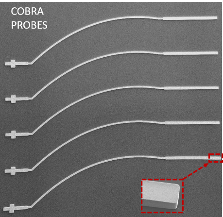
Xallent’s proprietary MEMS processing techniques are used to manufacture cobra probes. Probes could be assembled into full array, semi-array, staggered or peripheral probe card.
- Nano & Microfabrication: Fabrication expertise includes electron beam and photolithography, reactive ion etching (RIE), deep reactive ion etching (DRIE), ion milling, metal evaporation, and sputtering. Low-pressure chemical vapor deposition (LPCVD) is used for polysilicon, silicon-dioxide (SiO2), and nitride (Si3N4) thin films. Probe device release techniques include vapor HF, xenon-difluoride (XeF2), or buffered oxide etch (BOE) with critical point drying (CPD). SEM and AFM are used to inspect production prior to testing and packaging. Thin film stress characterization and other metrology techniques are used to increase the yield, reliability, and repeatability of probe device production.
- On-Wafer/Die Performance Testing: We test N/MEMS probe devices with a 3D optical profilometer to determine out-of-plane deflection of the released probe. We measure resonance frequency, phase, and amplitude with a laser Doppler vibrometer. Xallent probes, probe heads, wafer prober, and software are used for testing depending on the customer’s needs.
- Packaging: The wafer is typically diced using either a saw or a laser. Outsourced stealth dicing is available. The final die can be wire-bonded or flip-chip bonded to a preferred substrate such as ceramic or Printed Circuit Board (PCB). PCB designs are available to meet probe card specifications.
- Final Testing: Typical measurements include cycle, stress, and reliability tests. Final test results are certified prior to shipping.
Please note: Our manufacturing services extend to other NEMS and MEMS devices such as switches, microphones, mirrors, accelerometers, gyroscopes, pressure sensors, etc. Please contact us to learn more.
.
.
