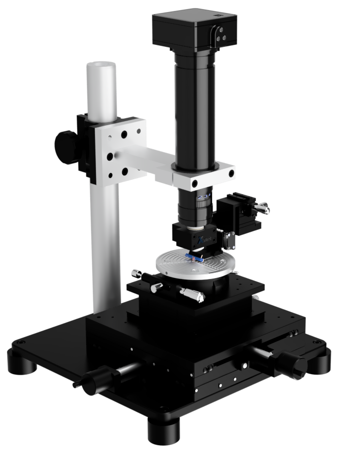
Sheet Resistance Test System
Gain early insights during new materials development
Sheet resistance provides insights into the electrical properties of conducting and semiconducting thin film materials. It is a measure of the resistance across a thin square of a material. Because it is independent of the size of the square, it serves as a good measure of comparing the electrical properties of different materials.
The SAKYIWA NanoProber is an entry level sheet resistance measurement test tool that utilizes our fine pitch four point probes (10 micron pitch) to directly measure the sheet resistance and resistivity of thin film materials. The micro and nanoscale resolution of our fine pitch four point probes make it possible to investigate how grain sizes, boundaries, defects, and material composition impact those measurements. Using that detailed information, researchers and production facilities can quickly optimize material production, reliability, and yields.
More tests, faster, with higher resolution and at a fraction of the cost, with a much smaller footprint than with conventional equipment


“Our Xallent system has given our user base several orders-of-magnitude improvement in measurement throughput and drastically decreased their cost of test. The Xallent system represents a key milestone in semiconductor and thin film materials characterization.”
Ron Olson
Director of Operations | Cornell NanoScale Facility
With an intuitive graphical user interface and analysis driven by computer vision, the SAKYIWA NanoProber software communicates with a source measure unit, piezo-controlled probe head, and camera to perform IV and sheet resistance measurements. A portfolio of our fine pitch probes (i.e., 4-point probes, parametric probes, and custom probes) can be used on the NanoProber. The NanoProber supports 100 mm wafers and pieces. Alternatively, the HITS-300 is an ideal semi-automatic test system for characterizing 300 mm and 200 mm wafers.
Applications
- IV
- Sheet resistance
- 4-wire Kelvin resistance
Specifications
- Supports 100 mm wafers and pieces
- Vision system with sub-2.5 µm resolution
- Accepts fine pitch probes
- Adjustable inline light intensity
- Leverages a high precision piezoelectric stage to bring probe tips into contact with wafer
Need additional information?
Let’s Talk
