 Skip to content
SAKYIWA NanoProber
High-Resolution Characterization. Minimal Footprint.
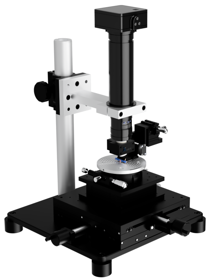
The next frontier in semiconductor, thin-film, LED, and photonics testing has arrived. The SAKYIWA NanoProber series delivers high-speed extraction of sheet resistance, 4-wire Kelvin resistance, and FET properties at the micro and nanoscale—all at a fraction of the cost and footprint of conventional equipment. The SAKYIWA NanoProber is engineered for surgical accuracy, featuring a computer-controlled piezoelectric Z-stage and dual manual XY stages. This high-precision assembly, integrated with a high-resolution vision system, allows for real-time viewing of the probe tips and the Material-Under-Test (MUT).
Driven by Xallent’s intuitive, computer-vision-powered software, the platform automates communication between the Source Measure Unit (SMU), piezo-stages, and camera. This seamless integration provides instantaneous generation of I/V curves, Kelvin resistance, sheet resistance, and transistor transfer/output characteristics.
More tests, faster, with higher resolution and at a fraction of the cost, with a much smaller footprint than with conventional equipment


“Our Xallent system has given our user base several orders-of-magnitude improvement in measurement throughput and drastically decreased their cost of test. The Xallent system represents a key milestone in semiconductor and thin film materials characterization.”
Ron Olson
Director of Operations | Cornell NanoScale Facility
A portfolio of our fine pitch probes (i.e., 4-point probes, parametric probes, and custom probes) can be used on the NanoProber. The NanoProber supports 100 mm wafers and pieces. Alternatively, the HITS™ is an ideal semi-automatic test system for characterizing 300 mm and 200 mm wafers.
Applications
- IV
- Sheet resistance
- 4-wire Kelvin resistance
- 2D FET output & transfer curve measurements
Specifications
- Supports 100 mm wafers and pieces
- Vision system with sub-2.5 µm resolution
- Accepts fine pitch probes
- Adjustable inline light intensity
- Leverages a high precision piezoelectric stage to bring probe tips into contact with wafer
Need additional information?
Let’s Talk
